


| Part Number(s) (NSID) |
Top View | Type | Pins | MSL Rating | Peak Reflow | RoHS Status |
CAD Symbols | Models | Package Marking Format |
|---|---|---|---|---|---|---|---|---|---|
| ADC08D1020CIYB/NOPB ADC08D1020CIYB |
LQFP EXP PAD | 128 | 3 3 |
260 260 |
Detail | Download | N/A |
NSUZXYYTTE# ADC08D1020 CIYB |
PDF
Description
The ADC08D1020 is a dual, low power, high performance, CMOS analog-to-digital converter that builds upon the ADC08D1000 platform. The ADC08D1020 digitizes signals to 8 bits of resolution at sample rates up to 1.3 GSPS. It has expanded features compared to the ADC08D1000, which include a test pattern output for system debug, a clock phase adjust, and selectable output demultiplexer modes. Consuming a typical 1.6 Watts in non-demultiplex mode at 1 GSPS from a single 1.9 Volt supply, this device is guaranteed to have no missing codes over the full operating temperature range. The unique folding and interpolating architecture, the fully differential comparator design, the innovative design of the internal sample-and-hold amplifier and the calibration schemes enable a very flat response of all dynamic parameters beyond Nyquist, producing a high 7.4 Effective Number of Bits (ENOB) with a 498 MHz input signal and a 1 GHz sample rate while providing a 10
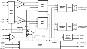
Each converter has a selectable output demultiplexer which feeds two LVDS buses. If the 1:2 demultiplexed mode is selected, the output data rate is reduced to half the input sample rate on each bus. When non-demultiplexed mode is selected, that output data rate on channels DI and DQ are at the same rate as the input sample clock. The two converters can be interleaved and used as a single 2 GSPS ADC.
The converter typically consumes less than 3.5 mW in the Power Down Mode and is available in a leaded or lead-free 128-lead, thermally enhanced, exposed pad, LQFP and operates over the Industrial (-40ЁуC
|
Resolution |
8 Bits |
|
Max Conversion Rate |
1 GSPS (min) |
|
Code Error Rate |
10 |
|
ENOB @ 498 MHz Input (Normal Mode) |
7.4 Bits (typ) |
|
DNL |
ЁР0.15 LSB (typ) |
Power Consumption
|
Operating in Non-demux Output |
1.6 W (typ) |
|
Operating in 1:2 Demux Output |
1.7 W (typ) |
|
Power Down Mode |
3.5 mW (typ) |
| • | Direct RF Down Conversion |
| • | Digital Oscilloscopes |
| • | Satellite Set-top boxes |
| • | Communications Systems |
| • | Test Instrumentation |
| • | Single +1.9V ЁР0.1V Operation |
| • | Interleave Mode for 2x Sample Rate |
| • | Multiple ADC Synchronization Capability |
| • | Adjustment of Input Full-Scale Range, Offset, and Clock Phase Adjust |
| • | Choice of SDR or DDR output clocking |
| • | 1:1 or 1:2 Selectable Output Demux |
| • | Second DCLK output |
| • | Duty Cycle Corrected Sample Clock |
| • | Test pattern |
Diagrams
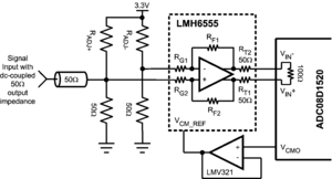
Typical Application
|
Block Diagram
|
Typical Performance 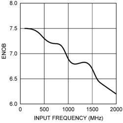 ENOB VS. INPUT FREQUENCY |
