


Description
The TPS1100 is a single P-channel enhancement-mode MOSFET. The device has been optimized for 3-V or 5-V power distribution in battery-powered systems by means of Texas Instruments LinBiCMOSTM process. With a maximum VGS(th) of -1.5 V and an IDSS of only 0.5 uA, the TPS1100 is the ideal high-side switch for low-voltage, portable battery-management systems where maximizing battery life is a primary concern. The low rDS(on) and excellent ac characteristics (rise time 10 ns typical) make the TPS1100 the logical choice for low-voltage switching applications such as power switches for pulse-width-modulated (PWM) controllers or motor/bridge drivers.
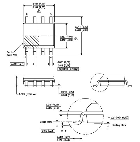
The ultrathin thin shrink small-outline package or TSSOP (PW) version with its smaller footprint and reduction in height fits in places where other P-channel MOSFETs cannot.
Features
- Low rDS(on) . . . 0.18
 Typ at VGS = -10 V
- 3 V Compatible
- Requires No External VCC
- TTL and CMOS Compatible Inputs
- VGS(th) = -1.5 V Max
- Available in Ultrathin TSSOP Package (PW)
- ESD Protection Up to 2 kV Per MIL-STD-883C, Method 3015
LinBICMOS is a trademark of Texas Instruments Incorporated
Pricing / Packaging
| Device | Status | Price | Quantity | Package | Pins | Top Side Marking | Package QTY | Package Carrier |
| TPS1100D | ACTIVE | 0.55 | 1ku | SOIC (D) | 8 | View | 75 | TUBE |
| TPS1100DG4 | ACTIVE | 0.55 | 1ku | SOIC (D) | 8 | View | 75 | TUBE |
| TPS1100DR | ACTIVE | 0.47 | 1ku | SOIC (D) | 8 | View | 2500 | LARGE T&R |
| TPS1100DRG4 | ACTIVE | 0.47 | 1ku | SOIC (D) | 8 | View | 2500 | LARGE T&R |
| TPS1100PW | ACTIVE | 0.55 | 1ku | TSSOP (PW) | 8 | View | 150 | TUBE |
| TPS1100PWG4 | ACTIVE | 0.55 | 1ku | TSSOP (PW) | 8 | View | 150 | TUBE |
| TPS1100PWLE | OBSOLETE | TSSOP (PW) | 8 | View | ||
| TPS1100PWR | ACTIVE | 0.47 | 1ku | TSSOP (PW) | 8 | View | 2000 | LARGE T&R |
| TPS1100PWRG4 | ACTIVE | 0.47 | 1ku | TSSOP (PW) | 8 | View | 2000 | LARGE T&R |
Packag
source⦿ShenZhen henlito electronic co.,ltd.
web:www.henlito.com
