


Replacement Device Characteristics Table
| Device | A120x Characteristics | ||||||
|---|---|---|---|---|---|---|---|
| BOP | BRP | Hys | |||||
| Legacy | Replacement | Min | Max | Min | Max | Min | Max |
| A1201 | A1205 | -40 | 50 | -50 | 40 | 5 | 55 |
| A1204 | A1203 | - | 95 | -95 | - | 30 | - |
| UGx3133 | A1202 | - | 75 | -75 | - | 30 | - |
| UGx3132 | A1203 | - | 95 | -95 | - | 30 | - |
| A3134 | A1205 | -40 | 50 | -50 | 40 | 5 | 55 |
Features and Benefits
- Continuous-time operation
- Fast power-on time
- Low noise
- Stable operation over full operating temperature range
- Reverse battery protection
- Solid-state reliability
- Factory-programmed at end-of-line for optimum performance
- Robust EMC performance
- High ESD rating
- Regulator stability without a bypass capacitor
Description
The Allegro® A1202 and A1203 Hall-effect bipolar switches are next-generation replacements and extension of the popular Allegro A3133 and A3132 bipolar switch product line. Overall, the A120x family, produced with BiCMOS technology, consists of continuous-time devices that feature fast power-on time and low-noise operation. Device programming is performed after packaging, to ensure increased switchpoint accuracy by eliminating offsets that can be induced by package stress. Unique Hall element geometries and low-offset amplifiers help to minimize noise and to reduce the residual offset voltage normally caused by device overmolding, temperature excursions, and thermal stress.
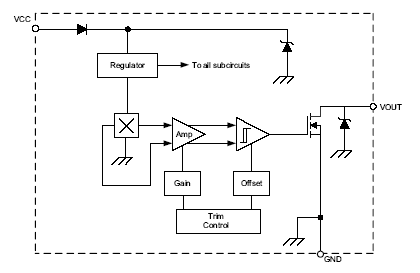
The A120x Hall-effect bipolar switches include the following on a single silicon chip: voltage regulator, Hall-voltage generator, small-signal amplifier, Schmitt trigger, and NMOS output transistor. The integrated voltage regulator permits operation from 3.8 to 24 V. The extensive on-board protection circuitry makes possible a \30 V absolute maximum voltage rating for superior protection in automotive and motor commutation applications, without adding external components. All devices in the family are identical, except for magnetic switchpoints.
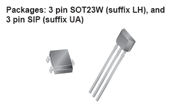
The small geometries of the BiCMOS process allow these devices to be provided in ultrasmall packages. The package styles available provide magnetically optimized solutions for most applications. Package LH is a SOT23W, a miniature low-profile surface-mount package, while package UA is a three-lead ultramini SIP for throughhole mounting. Each package is lead (Pb) free, with 100% matte tin plated leadframes.
Functional Block Diagram
source⦿ShenZhen henlito electronic co.,ltd.
web:www.henlito.com
