


| Part Number(s) (NSID) |
Top View | Type | Pins | MSL Rating | Peak Reflow | RoHS Status |
CAD Symbols | Models | Package Marking Format |
|---|---|---|---|---|---|---|---|---|---|
| LM2903ITL/NOPB |
 |
MICRO SMD | 8 | 1 | 260 | Detail | Download | N/A |
XVC I 03 |
| LM2903ITLX/NOPB |
|
MICRO SMD | 8 | 1 | 260 | Detail | Download | N/A |
XVC I 03 |
| LM2903M/NOPB LM2903M |
 |
SOIC NARROW | 8 | 1 1 |
260 235 |
Detail | Download | N/A |
NSZXTT LM 2903M |
| LM2903MX/NOPB LM2903MX |
|
SOIC NARROW | 8 | 1 1 |
260 235 |
Detail | Download | N/A |
NSZXTT LM 2903M |
| LM2903N/NOPB LM2903N |
 |
MDIP | 8 | 1 1 |
NA NA |
Detail | Download | N/A |
NSUZXYTTE# LM 2903N |
Description
The LM193 series consists of two independent precision voltage comparators with an offset voltage specification as low as 2.0 mV max for two comparators which were designed specifically to operate from a single power supply over a wide range of voltages. Operation from split power supplies is also possible and the low power supply current drain is independent of the magnitude of the power supply voltage. These comparators also have a unique characteristic in that the input common-mode voltage range includes ground, even though operated from a single power supply voltage.
Application areas include limit comparators, simple analog to digital converters; pulse, squarewave and time delay generators; wide range VCO; MOS clock timers; multivibrators and high voltage digital logic gates. The LM193 series was designed to directly interface with TTL and CMOS. When operated from both plus and minus power supplies, the LM193 series will directly interface with MOS logic where their low power drain is a distinct advantage over standard comparators.
The LM393 and LM2903 parts are available in National's innovative thin micro SMD package with 8 (12 mil) large bumps.
| • | High precision comparators |
| • | Reduced VOS drift over temperature |
| • | Eliminates need for dual supplies |
| • | Allows sensing near ground |
| • | Compatible with all forms of logic |
| • | Power drain suitable for battery operation |
- Wide supply
Voltage range:
2.0V to 36V
Single or dual supplies:
\1.0V to \18V
|
Very low supply current drain (0.4 mA) - independent of supply voltage |
|
|
Low input biasing current: |
25 nA |
|
Low input offset current: |
\5 nA |
|
Maximum offset voltage: |
\3 mV |
|
Input common-mode voltage range includes ground |
|
|
Differential input voltage range equal to the power supply voltage |
|
|
Low output saturation voltage,: |
250 mV at 4 mA |
|
Output voltage compatible with TTL, DTL, ECL, MOS and CMOS logic systems |
|
|
Available in the 8-Bump (12 mil) micro SMD package |
|
|
See AN-1112 for micro SMD considerations |
Diagrams
Typical Application
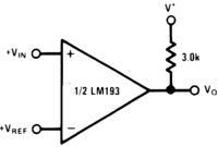
|
Connection Diagram
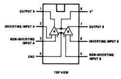
|
Typical Performance 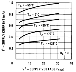 source⦿ShenZhen henlito electronic co.,ltd.
web:www.henlito.com |
