


description
The LPC2387 microcontroller is based on a 16-bit/32-bit ARM7TDMI-S CPU with real-time emulation that combines the microcontroller with 512 kB of embedded high-speed flash memory. A 128-bit wide memory interface and a unique accelerator architecture enable 32-bit code execution at the maximum clock rate. For critical performance in interrupt service routines and DSP algorithms, this increases performance up to 30 pct over Thumb mode. For critical code size applications, the alternative 16-bit Thumb mode reduces code by more than 30 pct with minimal performance penalty.
The LPC2387 is ideal for multi-purpose serial communication applications. It incorporates a 10/100 Ethernet Media Access Controller (MAC), USB full speed device with 4 kB of endpoint RAM, four UARTs, two CAN channels, an SPI interface, two Synchronous Serial Ports (SSP), three I2C interfaces, and an I2S interface. This blend of serial communications interfaces combined with an on-chip 4 MHz internal oscillator, 64 kB SRAM, 16 kB SRAM for Ethernet, 16 kB SRAM for USB and general purpose use, together with 2 kB battery powered SRAM makes this device very well suited for communication gateways and protocol converters. Various 32-bit timers, an improved 10-bit ADC, 10-bit DAC, one PWM unit, a CAN control unit, and up to 70 fast GPIO lines with up to 12 edge or level sensitive external interrupt pins make this microcontroller particularly suitable for industrial control and medical systems.
Features
- ARM7TDMI-S processor, running at up to 72 MHz.
- 512 kB on-chip flash program memory with In-System Programming (ISP) and In-Application Programming (IAP) capabilities. Flash program memory is on the ARM local bus for high performance CPU access.
- 64 kB of SRAM on the ARM local bus for high performance CPU access.
- 16 kB SRAM for Ethernet interface. Can also be used as general purpose SRAM.
- 16 kB SRAM for general purpose DMA use also accessible by USB.
- Dual Advanced High-performance Bus (AHB) system that provides for simultaneous Ethernet DMA, USB DMA, and program execution from on-chip flash with no contention between those functions. A bus bridge allows the Ethernet DMA to access the other AHB subsystem.
- Advanced Vectored Interrupt Controller (VIC), supporting up to 32 vectored interrupts.
- General Purpose DMA (GPDMA) on AHB controller that can be used with the SSP serial interfaces, the I2S port, and the Secure Digital/MultiMediaCard (SD/MMC) card port, as well as for memory-to-memory transfers.
- Serial interfaces:
- Ethernet MAC with associated DMA controller. These functions reside on an independent AHB.
- USB 2.0 device/host/OTG with on-chip PHY and associated DMA controller.
- Four UARTs with fractional baud rate generation, one with modem control I/O, one with IrDA support, all with FIFO.
- CAN controller with two channels.
- SPI controller.
- Two SSP controllers, with FIFO and multi-protocol capabilities. One is an alternate for the SPI port, sharing its interrupt and pins. These can be used with the GPDMA controller.
- Three I2C-bus interfaces (one with open-drain and two with standard port pins).
- I2S (Inter-IC Sound) interface for digital audio input or output. It can be used with the GPDMA.
- Other peripherals:
- SD/MMC memory card interface.
- 70 general purpose I/O pins with configurable pull-up/down resistors.
- 10-bit ADC with input multiplexing among 6 pins.
- 10-bit DAC.
- Four general purpose timers/counters with a total of 8 capture inputs and 10 compare outputs. Each timer block has an external count input.
- One PWM/timer block with support for three-phase motor control. The PWM has two external count inputs.
- Real-Time Clock (RTC) with separate power pin, clock source can be the RTC oscillator or the APB clock.
- 2 kB SRAM powered from the RTC power pin, allowing data to be stored when the rest of the chip is powered off.
- WatchDog Timer (WDT). The WDT can be clocked from the internal RC oscillator, the RTC oscillator, or the APB clock.
- Standard ARM test/debug interface for compatibility with existing tools.
- Emulation trace module supports real-time trace.
- Single 3.3 V power supply (3.0 V to 3.6 V).
- Three reduced power modes: idle, sleep, and power-down.
- Four external interrupt inputs configurable as edge/level sensitive. All pins on port 0 and port 2 can be used as edge sensitive interrupt sources.
- Processor wake-up from Power-down mode via any interrupt able to operate during Power-down mode (includes external interrupts, RTC interrupt, USB activity, Ethernet wake-up interrupt).
- Two independent power domains allow fine tuning of power consumption based on needed features.
- Each peripheral has its own clock divider for further power saving.
- Brownout detect with separate thresholds for interrupt and forced reset.
- On-chip power-on reset.
- On-chip crystal oscillator with an operating range of 1 MHz to 24 MHz.
- 4 MHz internal RC oscillator trimmed to 1 pct accuracy that can optionally be used as the system clock. When used as the CPU clock, does not allow CAN and USB to run.
- On-chip PLL allows CPU operation up to the maximum CPU rate without the need for a high frequency crystal. May be run from the main oscillator, the internal RC oscillator, or the RTC oscillator.
- Versatile pin function selections allow more possibilities for using on-chip peripheral functions.
Applications
- Industrial control
- Medical systems
- Protocol converter
- Communications
- Related applications
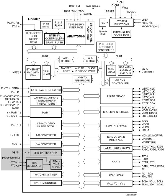
Block diagrams
web:www.henlito.com
