


| Part Number(s) (NSID) |
Top View | Type | Pins | MSL Rating | Peak Reflow | RoHS Status |
CAD Symbols | Models | Package Marking Format |
|---|---|---|---|---|---|---|---|---|---|
| LM2670S-12/NOPB LM2670S-12 |
 |
TO-263 | 7 | 3 3 |
245 235 |
Detail | Download | N/A |
NSUZXYTTE# LM2670 S-12 |
| LM2670S-3.3/NOPB LM2670S-3.3 |
|
TO-263 | 7 | 3 3 |
245 235 |
Detail | Download | N/A |
NSUZXYTTE# LM2670 S-3.3 |
| LM2670S-5.0/NOPB LM2670S-5.0 |
|
TO-263 | 7 | 3 3 |
245 235 |
Detail | Download | N/A |
NSUZXYTTE# LM2670 S-5.0 |
| LM2670S-ADJ/NOPB LM2670S-ADJ |
|
TO-263 | 7 | 3 3 |
245 235 |
Detail | Download | N/A |
NSUZXYTTE# LM2670 S-ADJ |
| LM2670SD-12/NOPB LM2670SD-12 |
 |
LLP | 14 | 1 1 |
260 260 |
Detail | Download | N/A |
NS UZXYTT S0002LB |
| LM2670SD-3.3/NOPB LM2670SD-3.3 |
|
LLP | 14 | 1 1 |
260 260 |
Detail | Download | N/A |
NS UZXYTT S0002NB |
| LM2670SD-5.0/NOPB LM2670SD-5.0 |
|
LLP | 14 | 1 1 |
260 260 |
Detail | Download | N/A |
NS UZXYTT S0002PB |
| LM2670SD-ADJ/NOPB LM2670SD-ADJ |
|
LLP | 14 | 1 1 |
260 260 |
Detail | Download | N/A |
NS UZXYTT S0002RB |
| LM2670SDX-12 |
|
LLP | 14 | 1 | 260 | Detail | Download | N/A |
NS UZXYTT S0002LB |
| LM2670SDX-3.3/NOPB |
|
LLP | 14 | 1 | 260 | Detail | Download | N/A |
NS UZXYTT S0002NB |
| LM2670SDX-5.0/NOPB |
|
LLP | 14 | 1 | 260 | Detail | Download | N/A |
NS UZXYTT S0002PB |
| LM2670SDX-ADJ/NOPB LM2670SDX-ADJ |
|
LLP | 14 | 1 1 |
260 260 |
Detail | Download | N/A |
NS UZXYTT S0002RB |
| LM2670SX-12/NOPB LM2670SX-12 |
|
TO-263 | 7 | 3 3 |
245 235 |
Detail | Download | N/A |
NSUZXYTTE# LM2670 S-12 |
| LM2670SX-3.3/NOPB LM2670SX-3.3 |
|
TO-263 | 7 | 3 3 |
245 235 |
Detail | Download | N/A |
NSUZXYTTE# LM2670 S-3.3 |
| LM2670SX-5.0/NOPB LM2670SX-5.0 |
|
TO-263 | 7 | 3 3 |
245 235 |
Detail | Download | N/A |
NSUZXYTTE# LM2670 S-5.0 |
| LM2670SX-ADJ/NOPB LM2670SX-ADJ |
|
TO-263 | 7 | 3 3 |
245 235 |
Detail | Download | N/A |
NSUZXYTTE# LM2670 S-ADJ |
| LM2670T-12/NOPB |
 |
TO-220 | 7 | 1 | NA | Detail | Download | N/A |
NSUZXYTTE# LM2670 T-12 |
| LM2670T-3.3/NOPB LM2670T-3.3 |
|
TO-220 | 7 | 1 1 |
NA NA |
Detail | Download | N/A |
NSUZXYTTE# LM2670 T-3.3 |
| LM2670T-5.0/NOPB LM2670T-5.0 |
|
TO-220 | 7 | 1 1 |
NA NA |
Detail | Download | N/A |
NSUZXYTTE# LM2670 T-5.0 |
| LM2670T-ADJ/NOPB LM2670T-ADJ |
|
TO-220 | 7 | 1 1 |
NA NA |
Detail | Download | N/A |
NSUZXYTTE# LM2670 T-ADJ |
PDF
Description
The LM2670 series of regulators are monolithic integrated circuits which provide all of the active functions for a step-down (buck) switching regulator capable of driving up to 3A loads with excellent line and load regulation characteristics. High efficiency (>90%) is obtained through the use of a low ON-resistance DMOS power switch. The series consists of fixed output voltages of 3.3V, 5V and 12V and an adjustable output version.
The SIMPLE SWITCHER concept provides for a complete design using a minimum number of external components. The switching clock frequency can be provided by an internal fixed frequency oscillator (260KHz) or from an externally provided clock in the range of 280KHz to 400Khz which allows the use of physically smaller sized components. A family of standard inductors for use with the LM2670 are available from several manufacturers to greatly simplify the design process. The external Sync clock provides direct and precise control of the output ripple frequency for consistent filtering or frequency spectrum positioning.
The LM2670 series also has built in thermal shutdown, current limiting and an ON/OFF control input that can power down the regulator to a low 50μA quiescent current standby condition. The output voltage is guaranteed to a \2% tolerance.
| • | Simple to design, high efficiency (>90%) step-down switching regulators |
| • | Efficient system pre-regulator for linear voltage regulators |
| • | Battery chargers |
| • | Communications and radio equipment regulator with synchronized clock frequency |
| • | Efficiency up to 94% |
| • | Simple and easy to design with (using off-the-shelf external components) |
| • | 150 mΩ DMOS output switch |
| • | 3.3V, 5V and 12V fixed output and adjustable (1.2V to 37V ) versions |
| • | 50μA standby current when switched OFF |
| • | \2%maximum output tolerance over full line and load conditions |
| • | Wide input voltage range: 8V to 40V |
| • | External Sync clock capability (280KHz to 400KHz) |
| • | 260 KHz fixed frequency internal oscillator |
| • | −40 to +125<C operating junction temperature range |
Diagrams
Typical Application
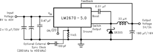
|
Block Diagram
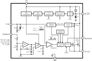
|
Typical Performance 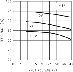 |
