Features
- High current 3-phase gate drive for N-channel MOSFETs
- Synchronous rectification
- Cross-conduction protection
- Charge pump and top-off charge pump for 100% PWM
- Integrated commutation decoder logic
- Operation over 5.5 to 50 V supply voltage range
- Extensive diagnostics output
- Provides +5 V Hall sensor power
- Low-current sleep mode
Description
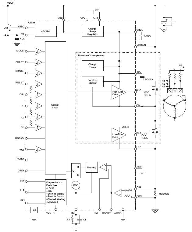
The A3930 and A3931 are 3-phase brushless dc (BLDC) motor controllers for use with N-channel external power MOSFETs. They incorporate much of the circuitry required to design a cost effective three-phase motor drive system, and have been specifically designed for automotive applications.
A key automotive requirement is functionality over a wide input supply range. A unique charge pump regulator provides adequate (>10 V) gate drive for battery voltages down to 7 V, and allows the device to operate with a reduced gate drive at battery voltages down to 5.5 V. Power dissipation in the charge pump is minimized by switching from a voltage doubling mode at low supply voltage to a dropout mode at the nominal running voltage of 14 V.
A bootstrap capacitor is used to provide the above-battery supply voltage required for N-channel MOSFETs. An internal charge pump for the high-side drive allows for dc (100% duty cycle) operation.
Internal fixed-frequency PWM current control circuitry can be used to regulate the maximum load current. The peak load current limit is set by the selection of an input reference voltage and external sensing resistor. The PWM frequency is set by a user-selected external RC timing network. For added flexibility, the PWM input can be used to provide speed and torque control, allowing the internal current control circuit to set the maximum current limit.
Efficiency is enhanced by using synchronous rectification. The power FETs are protected from shoot-through by integrated crossover control with dead time. The dead time can be set by a single external resistor.
The A3930 and A3931 only differ in their response to the all-zero combination on the Hall inputs. In this state, the A3930 indicates a logic fault, but the A3931 prepositions the motor in an unstable starting position suitable for start-up algorithms in microprocessordriven ^sensor-less ̄ control systems.
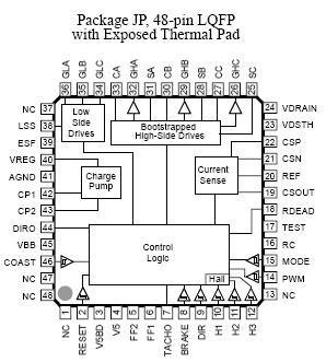
Both devices are supplied in a 48-pin LQFP with exposed thermal pad. This is a small footprint (81 mm2) power package, that is lead (Pb) free, with 100% matte tin leadframe plating.
Functional Block Diagram