


Features
- 2-wire serial I2C™-compatible interface: control (write) and status (read)
- LNB voltages (16 programmable levels) compatible with all common standards
- Tracking switch-mode power converter for lowest dissipation
- Integrated converter switches and current sensing
- Provides up to 500 mA per channel and 750 mA total
- Static current limit circuit allows full current at startup and 13★18 V output transition; reliably starts wide load range
- Push-pull output stage minimizes 13★18 V and 18★13 V output transition times for highly capacitive loads
- Adjustable rise/fall time via external timing capacitor
- Built-in tone oscillator, factory-trimmed to 22 kHz facilitates DiSEqC™ tone encoding, even at no-load
- Four methods of 22 kHz tone generation, via I2C™ data bits and/or external pin
- 22 kHz tone detector facilitates DiSEqC™ 2.0 decoding
- Auxiliary modulation input
- LNB overcurrent with timer
- Diagnostics for output voltage level, input supply UVLO, and DiSEqC™ tone output
- Cable disconnect diagnostic
Description
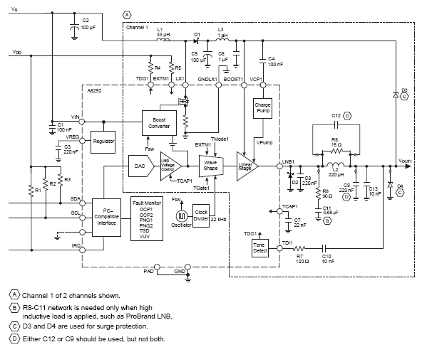
Intended for analog and digital satellite receivers, this dual low-noise block converter regulator (LNBR) is a monolithic linear and switching voltage regulator, specifically designed to provide the power and the interface signals to two LNB down converters via coaxial cables. The A8292 requires few external components, with the boost switches and compensation circuitry integrated inside of the device. A high switching frequency is chosen to minimize the size of the passive filtering components, further assisting in cost reduction. The high level of component integration ensures extremely low noise and ripple figures.
The A8292 has been designed for high efficiency, utilizing the Allegro® advanced BCD process. The integrated boost switches have been optimized to minimize both switching and static losses. To further enhance efficiency, the voltage drop across the tracking regulators has been minimized.
The A8292 has integrated tone detection capability, to support full two-way DiSEqC™ communications. Several schemes are available for generating tone signals, all the way down to no-load, and using either the internal clock or an external time source.
A comprehensive set of fault registers are provided which, comply with all the common standards, including: overcurrent, thermal shutdown, undervoltage, cable disconnect, power not good, and tone detect.
The device uses a 2-wire bidirectional serial interface, compatible with the I2C™ standard, that operates up to 400 kHz.
The A8292 is supplied in a lead (Pb) free 28-lead MLP/QFN with 100% matte tin leadframe plating.
Functional Block Diagram
source⦿ShenZhen henlito electronic co.,ltd.
web:www.henlito.com
