Industry's-First High-Performance Boost Regulator with Dual Charge-Pump Regulators for Small-Sized Battery-Powered LCD Applications
| Status |
| Active: In Production. |
| Description | ||||||
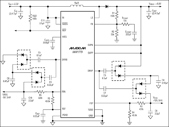
The primary high-power DC-DC converter generates a boosted output voltage (VMAIN) up to 13V that is regulated within \1%. The low-power BiCMOS control circuitry and the low on-resistance (1 ohm) of the integrated power MOSFET allows efficiency up to 91%. The 250kHz current-mode pulse-width modulation (PWM) architecture provides fast transient response and allows the use of ultra-small inductors and ceramic capacitors. The dual charge pumps independently regulate one positive output (VPOS) and one negative output (VNEG). These low-power outputs use external diode and capacitor stages (as many stages as required) to regulate output voltages up to +40V and down to -40V. A proprietary regulation algorithm minimizes output ripple, as well as capacitor sizes for both charge pumps. The MAX1779 is available in the ultra-thin TSSOP package (1.1mm max height). | ||||||
| Key Specifications: Multifunction PMICs | ||||||||||||||||||||||||||||||
| Part Number | Primary Topology | Monitor/Control Features | DC-DC/Power Features | LCD/LED/Flash/CCD Features | VIN (V) |
VIN (V) |
VOUT (V) |
VOUT (V) |
Max. IOUT (A) |
Max. IOUT (A) |
Oper. Freq. (kHz) |
Package/Pins | Smallest Available Pckg. (mm2) |
Price | ||||||||||||||||
| min | max | min | max | − | + | max w/pins | See Notes | |||||||||||||||||||||||
| MAX1779 | Step-Up | Shutdown |
|
TFT Bias | 2.7 | 5.5 | 2.7 | 13 | 0.18 | 0.18 | 250 |
|
33.4 | $2.89 @1k | ||||||||||||||||
| See All Multifunction PMICs (83) | ||||||||||||||||||||||||||||||
| Diagram |
 Typical Operating Circuit |
source⦿ShenZhen henlito electronic co.,ltd.
web:www.henlito.com


 Download