


Pricing / Packaging
| Device | Status | Temp (oC) | Price | Quantity | Package | Pins | Top Side Marking | Package QTY | Package Carrier |
| SN74ALS112AD | ACTIVE | 0 to 70 | 0.85 | 1ku | SOIC (D) | 16 | View | 40 | TUBE |
| SN74ALS112ADE4 | ACTIVE | 0 to 70 | 0.85 | 1ku | SOIC (D) | 16 | View | 40 | TUBE |
| SN74ALS112ADG4 | ACTIVE | 0 to 70 | 0.85 | 1ku | SOIC (D) | 16 | View | 40 | TUBE |
| SN74ALS112ADR | ACTIVE | 0 to 70 | 0.75 | 1ku | SOIC (D) | 16 | View | 2500 | LARGE T&R |
| SN74ALS112ADRE4 | ACTIVE | 0 to 70 | 0.75 | 1ku | SOIC (D) | 16 | View | 2500 | LARGE T&R |
| SN74ALS112ADRG4 | ACTIVE | 0 to 70 | 0.75 | 1ku | SOIC (D) | 16 | View | 2500 | LARGE T&R |
| SN74ALS112AN | ACTIVE | 0 to 70 | 0.85 | 1ku | PDIP (N) | 16 | View | 25 | TUBE |
| SN74ALS112AN3 | OBSOLETE | 0 to 70 | PDIP (N) | 16 | View | ||
| SN74ALS112ANE4 | ACTIVE | 0 to 70 | 0.85 | 1ku | PDIP (N) | 16 | View | 25 | TUBE |
| SN74ALS112ANSR | ACTIVE | 0 to 70 | 0.85 | 1ku | SO (NS) | 16 | View | 2000 | LARGE T&R |
| SN74ALS112ANSRE4 | ACTIVE | 0 to 70 | 0.85 | 1ku | SO (NS) | 16 | View | 2000 | LARGE T&R |
| SN74ALS112ANSRG4 | ACTIVE | 0 to 70 | 0.85 | 1ku | SO (NS) | 16 | View | 2000 | LARGE T&R |
Description
These devices contain two independent J-K negative-edge-triggered flip-flops. A low level at the preset (![]() ) or clear (
) or clear (![]() ) inputs sets or resets the outputs, regardless of the levels of the other inputs. When
) inputs sets or resets the outputs, regardless of the levels of the other inputs. When ![]() and
and ![]() are inactive (high), data at the J and K inputs meeting the setup-time requirements is transferred to the outputs on the negative-going edge of the clock pulse (CLK). Clock triggering occurs at a voltage level and is not directly related to the fall time of the clock pulse. Following the hold-time interval, data at the J and K inputs may be changed without affecting the levels at the outputs. These versatile flip-flops can perform as toggle flip-flops by tying J and K high.
are inactive (high), data at the J and K inputs meeting the setup-time requirements is transferred to the outputs on the negative-going edge of the clock pulse (CLK). Clock triggering occurs at a voltage level and is not directly related to the fall time of the clock pulse. Following the hold-time interval, data at the J and K inputs may be changed without affecting the levels at the outputs. These versatile flip-flops can perform as toggle flip-flops by tying J and K high.
The SN54ALS112A is characterized for operation over the full military temperature range of -55<C to 125<C.
Features
- Fully Buffered to Offer Maximum Isolation From External Disturbance
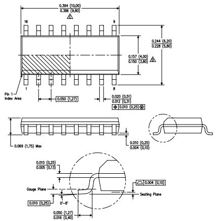
- Package Options Include Plastic Small-Outline (D) Packages, Ceramic Chip Carriers (FK), and Standard Plastic (N) and Ceramic (J) 300-mil DIPs
Packaging
source⦿ShenZhen henlito electronic co.,ltd.
web:www.henlito.com
