Pricing, Packaging
| Model | Status | Package | Pins | Temp. Range |
Price* (100-499) |
Price* (1000 pcs.) |
Production** Availability |
ROHS Compliant |
|---|---|---|---|---|---|---|---|---|
| AD5544ARS | Prodn | 28 ld SSOP | 28 | Ind | $24.10 | $19.75 | 02/26/2010 | N Material Declaration |
| AD5544ARSZ | Prodn | 28 ld SSOP | 28 | Ind | $20.61 | $16.89 | 02/26/2010 | Y Material Declaration |
| AD5544ARSZ-REEL7 | Prodn | 28 ld SSOP | 28 | Ind | - | $17.10 | - | Y Material Declaration |
| AD5544BRSZ | Prodn | 28 ld SSOP | 28 | Ind | $23.78 | $19.49 | 02/26/2010 | Y Material Declaration |
| AD5544BRSZ-REEL7 | Prodn | 28 ld SSOP | 28 | Ind | - | $19.49 | - | Y Material Declaration |
Description
The AD5544/AD5554 quad, 16-/14-bit, current output, digital-to-analog converters (DACs) are designed to operate from 2.7 V to 5.5 V supply range.
The applied external reference input voltage (VREF) determines the full-scale output current. Integrated feedback resistors (RFB) provide temperature-tracking, full-scale voltage outputs when combined with an external I-to-V precision amplifier.
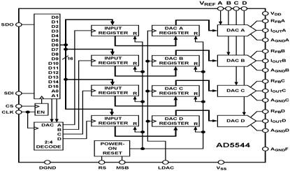
A double-buffered serial data interface offers high speed, 3-wire, SPI- and microcontroller-compatible inputs using serial data in (SDI), a chip select (CS), and clock (CLK) signals. In addition, a serial data out pin (SDO) allows for daisy-chaining when multiple packages are used. A common, level-sensitive, load DAC strobe (LDAC) input allows the simultaneous update of all DAC outputs from previously loaded input registers. Additionally, an internal power-on reset forces the output voltage to 0 at system turn-on. An MSB pin allows system reset assertion (RS) to force all registers to zero code when MSB = 0, or to half-scale code when MSB = 1.
The AD5544/AD5554 are packaged in the compact 28-lead SSOP.
Applications
- Automatic test equipment
- Instrumentation
- Digitally controlled calibration
Features
INL of \1 LSB (B Grade)
INL of \2 LSB (A Grade)
AD5544 Functional Block Diagram

AD5544 Functional Block Diagram
source⦿ShenZhen henlito electronic co.,ltd.
web:www.henlito.com


