Replacement Device Characteristics Table
| Device | A130x Characteristics | |||
|---|---|---|---|---|
| Typical Sensitivity | Operating Voltage | |||
| Legacy | Replacement | Min | Max | |
| - | A1301 | 2.5 mV/G | 4.5 V | 6 V |
| UGN3503 | A1302 | 1.3 mV/G | 4.5 V | 6 V |
Features and Benefits
- Low-noise output
- Fast power-on time
- Ratiometric rail-to-rail output
- 4.5 to 6.0 V operation
- Solid-state reliability
- Factory-programmed at end-of-line for optimum performance
- Robust ESD performance
Description
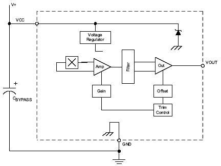
The A1301 and A1302 are continuous-time, ratiometric, linear Hall-effect sensor ICs. They are optimized to accurately provide a voltage output that is proportional to an applied magnetic field. These devices have a quiescent output voltage that is 50% of the supply voltage. Two output sensitivity options are provided: 2.5 mV/G typical for the A1301, and 1.3 mV/G typical for the A1302.
The Hall-effect integrated circuit included in each device includes a Hall sensing element, a linear amplifier, and a CMOS Class A output structure. Integrating the Hall sensing element and the amplifier on a single chip minimizes many of the problems normally associated with low voltage level analog signals.
High precision in output levels is obtained by internal gain and offset trim adjustments made at end-of-line during the manufacturing process.
These features make the A1301 and A1302 ideal for use in position sensing systems, for both linear target motion and rotational target motion. They are wellsuited for industrial applications over extended temperature ranges, from -40<C to 125<C.
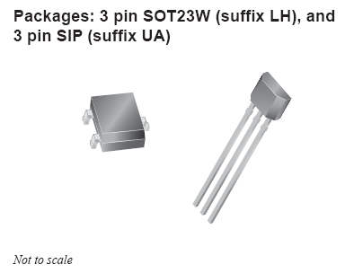
Two device package types are available: LH, a 3-pin SOT23W type for surface mount, and UA, a 3-pin ultramini SIP for through-hole mount. Each package is available in a lead (Pb) free version (suffix, -T) with 100% matte tin plated leadframe.
Functional Block Diagram