The A1321 and A1323 devices are intended to replace the A3515/7 and A3516/8 devices respectively. It is recommended that these new devices be used for all new designs.
Features and Benefits
- Temperature-stable quiescent output voltage
- Precise recoverability after temperature cycling
- Output voltage proportional to magnetic flux density
- Ratiometric rail-to-rail output
- Improved sensitivity
- 4.5 to 5.5 V operation
- Immune to mechanical stress
- Solid-state reliability
- Robust EMC protection
Description
The A132X family of linear Hall-effect sensor ICs are optimized, sensitive, and temperature-stable. These ratiometric Hall-effect sensor ICs provide a voltage output that is proportional to the applied magnetic field. The A132X family has a quiescent output voltage that is 50% of the supply voltage and output sensitivity options of 2.5 mV/G, 3.125 mV/G, and 5 mV/G. The features of this family of devices are ideal for use in the harsh environments found in automotive and industrial linear and rotary position sensing systems.
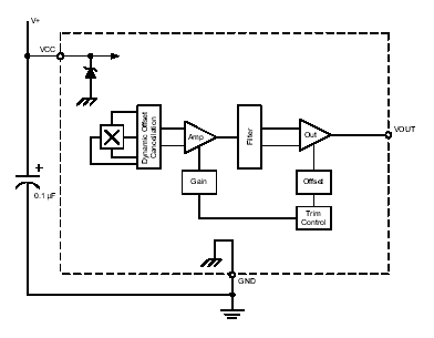
Each device has a BiCMOS monolithic circuit which integrates a Hall element, improved temperature-compensating circuitry to reduce the intrinsic sensitivity drift of the Hall element, a small-signal high-gain amplifier, and a rail-to-rail low-impedance output stage.
A proprietary dynamic offset cancellation technique, with an internal high-frequency clock, reduces the residual offset voltage normally caused by device overmolding, temperature dependencies, and thermal stress. The high frequency clock allows for a greater sampling rate, which results in higher accuracy and faster signal processing capability. This technique produces devices that have an extremely stable quiescent output voltage, are immune to mechanical stress, and have precise recoverability after temperature cycling. Having the Hall element and an amplifier on a single chip minimizes many problems normally associated with low-level analog signals.
Output precision is obtained by internal gain and offset trim adjustments made at end-of-line during the manufacturing process.
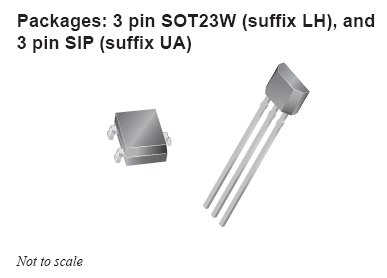
The A132X family is provided in a 3-pin single in-line package (UA) and a 3-pin surface mount package (LH). Each package is available in a lead (Pb) free version (suffix, –T) , with a 100% matte tin plated leadframe.
Functional Block Diagram