| Part Number(s) (NSID) |
Top View | Type | Pins | MSL Rating | Peak Reflow | RoHS Status |
CAD Symbols | Models | Package Marking Format |
|---|---|---|---|---|---|---|---|---|---|
| ADC08D1520CIYB/NOPB ADC08D1520CIYB |
LQFP EXP PAD | 128 | 3 3 |
260 260 |
Detail | Download | adc08d1520ciyb.ibs |
NSUZXYYTTE# ADC08D1520 CIYB |
Description
The ADC08D1520 is a dual, low power, high performance CMOS analog-to-digital converter that builds upon the
Each converter has a selectable output demultiplexer which feeds two LVDS buses. If the 1:2 Demultiplexed Mode is selected, the output data rate is reduced to half the input sample rate on each bus. When Non-Demultiplexed Mode is selected, the output data rate on channels DI and DQ is at the same rate as the input sample clock. The two converters can be interleaved and used as a single 3 GSPS ADC.
The converter typically consumes less than 3.5 mW in the Power Down Mode and is available in a leaded or lead-free, 128-pin, thermally enhanced, exposed pad, LQFP and operates over the Industrial (-40<C
|
Resolution |
8 Bits |
|
Max Conversion Rate |
1.5 GSPS (max) |
|
Code Error Rate |
10 |
|
ENOB @ 748 MHz Input |
7.4 Bits (typ) |
|
DNL |
\0.15 LSB (typ) |
|
Operating in Non-demux Mode |
1.6 W (typ) |
|
Operating in 1:2 Demux Mode |
2.0 W (typ) |
|
Power Down Mode |
3.5 mW (typ) |
| • | Direct RF Down Conversion |
| • | Digital Oscilloscopes |
| • | Satellite Set-top boxes |
| • | Communications Systems |
| • | Test Instrumentation |
| • | Single +1.9V \0.1V Operation |
| • | Interleave Mode for 2x Sample Rate |
| • | Multiple ADC Synchronization Capability |
| • | Adjustment of Input Full-Scale Range, Clock Phase, and Offset |
| • | Choice of SDR or DDR Output Clocking |
| • | 1:1 or 1:2 Selectable Output Demux |
| • | Second DCLK Output |
| • | Duty Cycle Corrected Sample Clock |
| • | Test pattern |
Diagrams
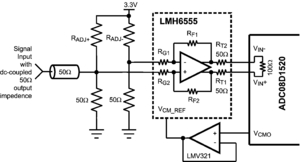
Typical Application

|
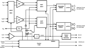
Block Diagram

|
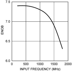
Typical Performance  ENOB vs INPUT FREQUENCY
|


