


| Part Number(s) (NSID) |
Top View | Type | Pins | MSL Rating | Peak Reflow | RoHS Status |
CAD Symbols | Models | Package Marking Format |
|---|---|---|---|---|---|---|---|---|---|
| ADC08D500CIYB/NOPB ADC08D500CIYB |
LQFP EXP PAD | 128 | 3 3 |
260 260 |
Detail | Download | adc08d500.ibs |
NSUZXYYTTE# ADC08D500 CIYB |
PDF
Description
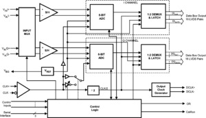
The ADC08D500 is a dual, low power, high performance CMOS analog-to-digital converter that digitizes signals to 8 bits resolution at sampling rates up to 800 MSPS. Consuming a typical 1.4 Watts at 500 MSPS from a single 1.9 Volt supply, this device is guaranteed to have no missing codes over the full operating temperature range. The unique folding and interpolating architecture, the fully differential comparator design, the innovative design of the internal sample-and-hold amplifier and the self-calibration scheme enable a very flat response of all dynamic parameters beyond Nyquist, producing a high 7.5 ENOB with a 250 MHz input signal and a 500 MHz sample rate while providing a 10
Each converter has a 1:2 demultiplexer that feeds two LVDS buses and reduces the output data rate on each bus to half the sampling rate. The two converters can be interleaved and used as a single 1 GSPS ADC.
The converter typically consumes less than 3.5 mW in the Power Down Mode and is available in a 128-lead, thermally enhanced exposed pad LQFP and operates over the Industrial (-40<C
|
Resolution |
8 Bits |
|
Max Conversion Rate |
500 MSPS (min) |
|
Bit Error Rate |
10 |
|
ENOB @ 250 MHz Input |
7.5 Bits (typ) |
|
DNL |
\0.15 LSB (typ) |
|
Power Consumption |
|
Operating |
1.4 W (typ) |
|
Power Down Mode |
3.5 mW (typ) |
| • | Direct RF Down Conversion |
| • | Digital Oscilloscopes |
| • | Satellite Set-top boxes |
| • | Communications Systems |
| • | Test Instrumentation |
| • | Internal Sample-and-Hold |
| • | Single +1.9V \0.1V Operation |
| • | Choice of SDR or DDR output clocking |
| • | Interleave Mode for 2x Sampling Rate |
| • | Multiple ADC Synchronization Capability |
| • | Guaranteed No Missing Codes |
| • | Serial Interface for Extended Control |
| • | Fine Adjustment of Input Full-Scale Range and Offset |
| • | Duty Cycle Corrected Sample Clock |
Diagrams
|
|
Block Diagram
|
Typical Performance 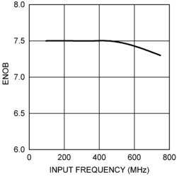
|
