


| Part Number(s) (NSID) |
Top View | Type | Pins | MSL Rating | Peak Reflow | RoHS Status |
CAD Symbols | Models | Package Marking Format |
|---|---|---|---|---|---|---|---|---|---|
| ADC10D1500CIUT/NOPB ADC10D1500CIUT |
TEPBGA | 292 | 3 3 |
250 220 |
Detail | N/A | N/A |
NSUZXYYTTE# ADC10D1500 CIUT |
PDF
Description
The ADC10D1000/1500 is the latest advance in National's Ultra-High-Speed ADC family. This low-power, high-performance CMOS analog-to-digital converter digitizes signals at 10-bit resolution for dual channels at sampling rates of up to 1.0/1.5 GSPS (Non-DES Mode) or for a single channel up to 2.0/3.0 GSPS (DES Mode). The ADC10D1000/1500 achieves excellent accuracy and dynamic performance while dissipating less than 2.8/3.6 Watts. The product is packaged in a leaded or lead-free 292-ball thermally enhanced BGA package over the rated industrial temperature range of
The ADC10D1000/1500 builds upon the features, architecture and functionality of the 8-bit GHz family of ADCs. An expanded feature set includes AutoSync for multi-chip synchronization,
Each channel has its own independent DDR Data Clock, DCLKI and DCLKQ, which are in phase when both channels are powered up, so that only one Data Clock could be used to capture all data, which is sent out at the same rate as the input sample clock. If the 1:2 Demux Mode is selected, a second 10-bit LVDS bus becomes active for each channel, such that the output data rate is sent out two times slower to relax data-capture timing requirements. The part can also be used as a single 2.0/3.0 GSPS ADC to sample one of the I or Q inputs. The output formatting can be programmed to be offset binary or two's complement and the Low Voltage Differential Signaling (LVDS) digital outputs are compatible with IEEE 1596.3-1996, with the exception of an adjustable common mode voltage between 0.8V and 1.2V to allow for power reduction for well-controlled back planes.
(Non-Demux Non-DES Mode, Fs=1.0/1.5 GSPS, Fin = 100 MHz)
|
Resolution |
10 Bits |
Conversion Rate
|
Dual channels at 1.0/1.5 GSPS (typ) |
|
Single channel at 2.0/3.0 GSPS (typ) |
|
Code Error Rate |
10 |
|
ENOB |
9.1/9.0 bits (typ) |
|
SNR |
57/56.8 dB (typ) |
|
SFDR |
70/68 dBc (typ) |
|
Full Power Bandwidth |
2.8/3.1 GHz (typ) |
|
DNL |
\0.25/\0.25 LSB (typ) |
Power Consumption
|
Single Channel Enabled |
1.61/1.92W (typ) |
|
Dual Channels Enabled |
2.77/3.59W (typ) |
|
Power Down Mode |
6/6 mW (typ) |
| • | Wideband Communications |
| • | Data Acquisition Systems |
| • | Digital Oscilloscopes |
| • | Excellent accuracy and dynamic performance |
| • | Low power consumption, further reduced at lower Fs |
| • | Internally terminated, buffered, differential analog inputs |
| • | R/W SPI Interface for Extended Control Mode |
| • | Dual-Edge Sampling Mode, in which the I- and Q-channels sample one input at twice the sampling clock rate |
| • | Test patterns at output for system debug |
| • | Programmable 15-bit gain and 12-bit plus sign offset |
| • | Programmable tAD adjust feature |
| • | 1:1 non-demuxed or 1:2 demuxed LVDS outputs |
| • | AutoSync feature for multi-chip systems |
| • | Single 1.9V \ 0.1V power supply |
| • | 292-ball BGA package (27mm x 27mm x 2.4mm with 1.27mm ball-pitch); no heat sink required |
| • | LC sampling clock filter for jitter reduction |
Diagrams
Typical Application
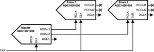
AutoSync diagramBlock Diagram

Block Diagram
Typical Performance
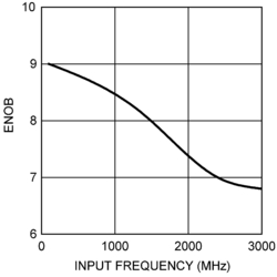
ENOB vs Fin
