


| Part Number(s) (NSID) |
Top View | Type | Pins | MSL Rating | Peak Reflow | RoHS Status |
CAD Symbols | Models | Package Marking Format |
|---|---|---|---|---|---|---|---|---|---|
| ADC10D1000CCMLS |
CCGA | 376 | 1 | NA | Detail | N/A | adc10d1000qml.ibs |
NSZSSXXYYA ADC10D1000CC MLS |
PDF
Description
The ADC10D1000 is the latest advance in National's Ultra-High-Speed ADC family of products. This low-power, high-performance CMOS analog-to-digital converter digitizes signals at 10-bit resolution at sampling rates of up to 1.0 GSPS in dual channel mode or 2.0 GSPS in single channel mode. The ADC10D1000 achieves excellent accuracy and dynamic performance while consuming a typical 2.9 Watts of power. This space grade, Radiation Tolerant part is rad hard to a single event latch up level of greater than 120MeV and a total dose (TID) of 100 krad(Si). The product is packaged in a hermatic 376 column thermally enhanced CCGA package rated over the temperature range of
The ADC10D1000 builds upon the features, architecture and functionality of the 8-bit GHz family of ADCs. New features include an auto-sync feature for multi-chip synchronization, independent programmable
Each channel has its own independent DDR Data Clock, DCLKI and DCLKQ, which are in phase when both channels are powered up, so that only one Data Clock could be used to capture all data, which is sent out at the same rate as the input sample clock. If the 1:2 Demultiplexed Mode is selected, a second 10-bit LVDS bus becomes active for each channel, such that the output data rate is sent out two times slower, but two times wider to relax data-capture timing margin. The two channels (I and Q) can also be interleaved (DES Mode) and used as a single 2.0 GSPS ADC to sample on the Q input. The output formatting is offset binary or two's complement and the Low Voltage Differential Signaling (LVDS) digital outputs are compatible with IEEE 1596.3-1996, with the exception of an adjustable common mode voltage between 0.8V and 1.2V.
(Non-Demux Non-DES Mode, Fs = 1.0 GSPS, Fin = 248 MHz)
|
Resolution |
10 Bits |
Conversion Rate
|
Dual channels at 1.0 GSPS (typ) |
|
Single channel at 2.0 GSPS (typ) |
|
Code Error Rate |
10 |
|
ENOB |
9.0 bits (typ) |
|
SNR |
56.1 dBc (typ) |
|
SFDR |
63 dBc (typ) |
|
Full Power Bandwidth |
2.8 GHz (typ) |
|
DNL |
\0.2 LSB (typ) |
Power Consumption
|
Single Channel Enabled |
1.64W (typ) |
|
Dual Channels Enabled |
2.9W (typ) |
|
Power Down Mode |
6 mW (typ) |
| • | Data Acquisition Systems |
| • | Wideband Communications |
| • | Direct RF Down Conversion |
|
Total Ionizing Dose |
100 krad(Si) |
|
Single Event Latch-up |
120 Mev-cm |
Excellent accuracy and dynamic performance
Diagrams
Typical Application
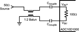 ac coupling input balun circuit
|
Block Diagram
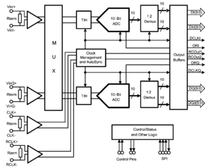 Block Diagram
|
Typical Performance 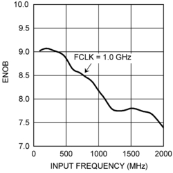 ENOB vs. INPUT FREQUENCY
|
