| Status |
| Active: In Production. |
| Description | ||||||
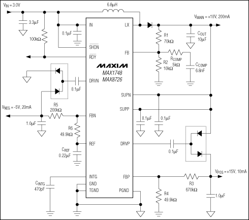
The primary 1MHz DC-DC converter generates a boosted output voltage (VMAIN) up to 13V using ultra-small inductors and ceramic capacitors. The low-power BiCMOS control circuitry and the low on-resistance (0.35Ω) of the integrated power MOSFET allows efficiency up to 93%. The dual charge pumps independently regulate one positive output (VPOS) and one negative output (VNEG). These low-power outputs use external diode and capacitor stages (as many stages as required) to regulate output voltages up to +40V and down to -40V. A proprietary regulation algorithm minimizes output ripple, as well as capacitor sizes for both charge pumps. For both the MAX1748 and MAX8726, the supply sequence is VMAIN first, VNEG next, and finally VPOS. The MAX1748 soft-starts each supply as soon as the previous supply finishes. The MAX8726 adds a delay between the startups of VMAIN and VNEG and also between VNEG and VPOS. The MAX1748/MAX8726 are available in the ultra-thin TSSOP package (1.1mm max height). | ||||||
An evaluation kit is available: MAX1748EVKIT
| Key Specifications: Multifunction PMICs | ||||||||||||||||||||||||||||||
| Part Number | Primary Topology | Monitor/Control Features | DC-DC/Power Features | LCD/LED/Flash/CCD Features | VIN (V) |
VIN (V) |
VOUT (V) |
VOUT (V) |
Max. IOUT (A) |
Max. IOUT (A) |
Oper. Freq. (kHz) |
Package/Pins | Smallest Available Pckg. (mm2) |
Price | ||||||||||||||||
| min | max | min | max | − | + | max w/pins | See Notes | |||||||||||||||||||||||
| MAX1748 | Step-Up | Shutdown |
|
TFT Bias | 2.7 | 5.5 | 2.7 | 13 | 0.5 | 0.5 | 1000 |
|
33.4 | $3.07 @1k | ||||||||||||||||
| See All Multifunction PMICs (83) | ||||||||||||||||||||||||||||||
| Diagram |
 Typical Operating Circuit |
source⦿ShenZhen henlito electronic co.,ltd.
web:www.henlito.com


 Download